
Semiconductor Physical Design & Analog Layout Engineering | Bangalore, India
High-precision chip design, custom physical implementation, and sign-off verification for global technology leaders.
Specialized Engineering Services
Comprehensive RTL-to-GDSII solutions across advanced process nodes.
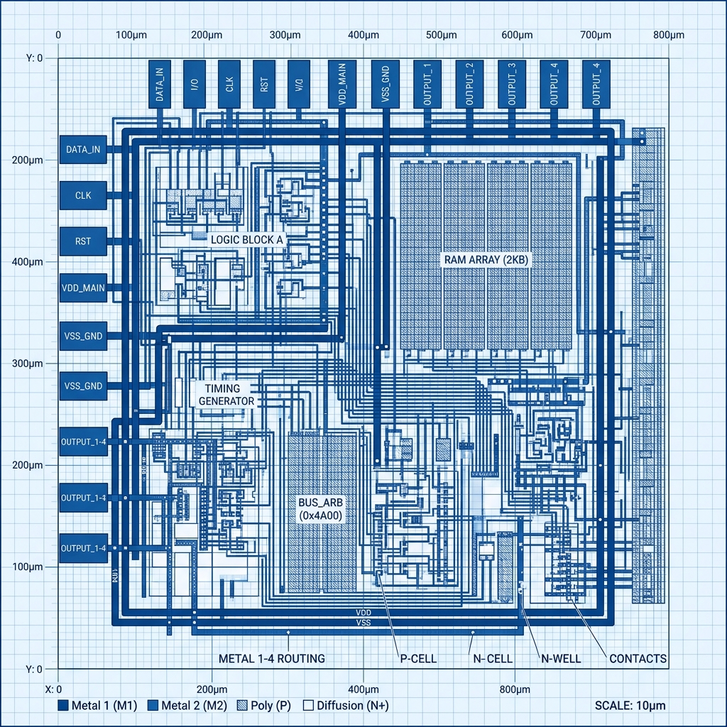
Physical Design
Complete RTL-to-GDSII flow including floorplanning, placement, CTS, and detailed routing for complex SoCs.
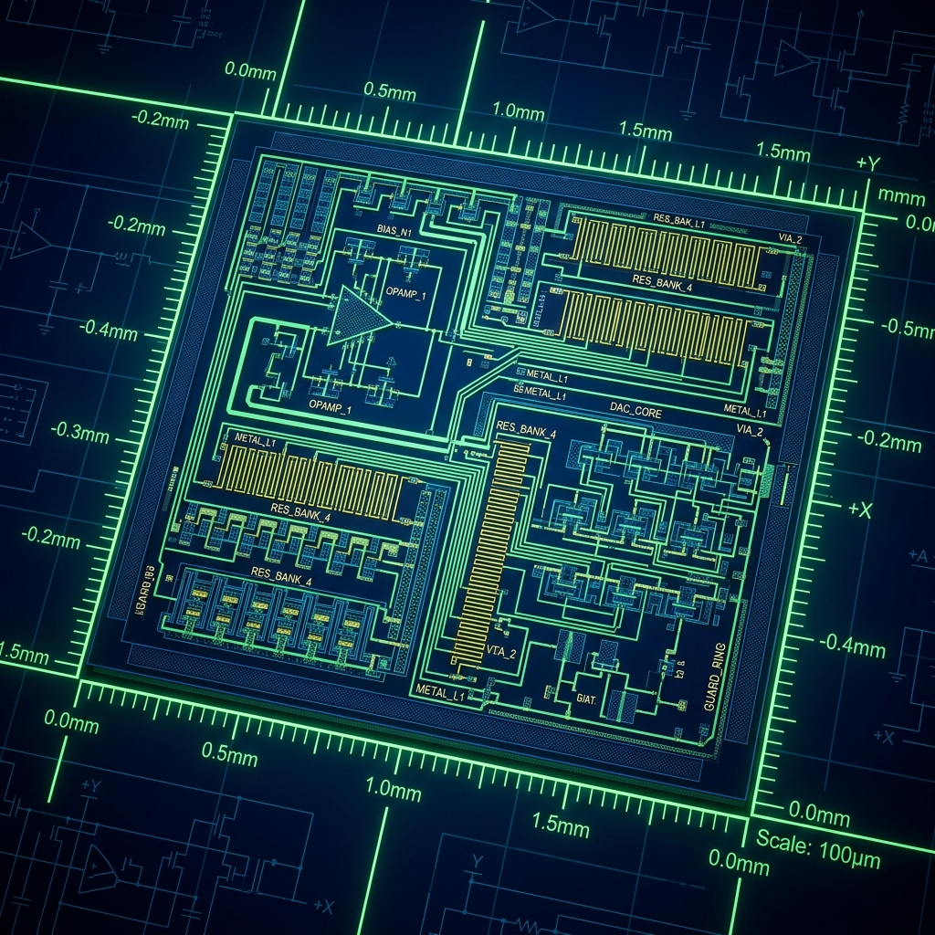
Analog Layout
High-precision custom analog layouts for SerDes, PLLs, DAC/ADC, and power management modules.
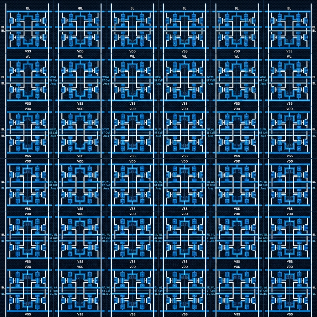
Memory Layout
Custom bitcell layout, sensing circuitry, and optimized memory compilers for performance and density.
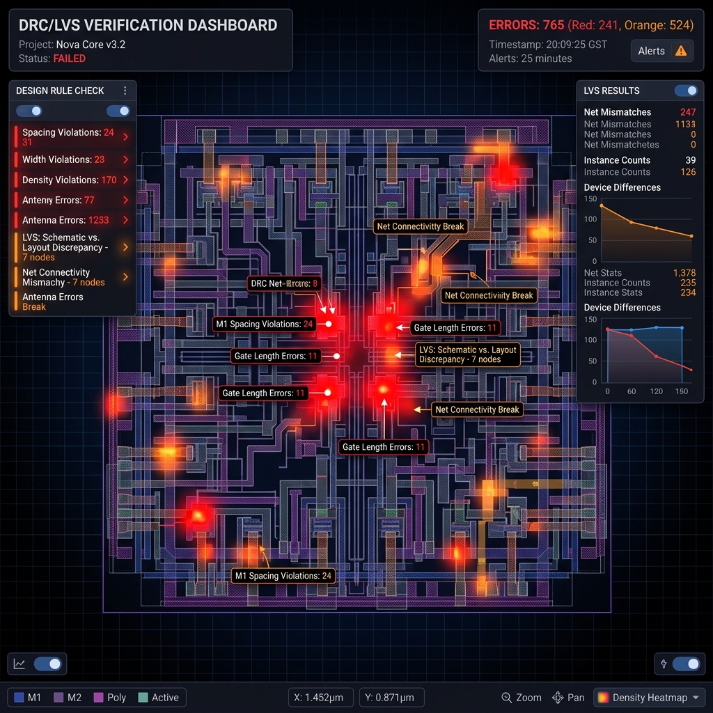
Physical Verification
Comprehensive DRC, LVS, and Antenna checks across advanced process nodes to ensure first-pass success.
EMIR Analysis
Exhaustive power integrity analysis, IR drop mitigation, and electromigration checks for device reliability.
Static Timing Analysis
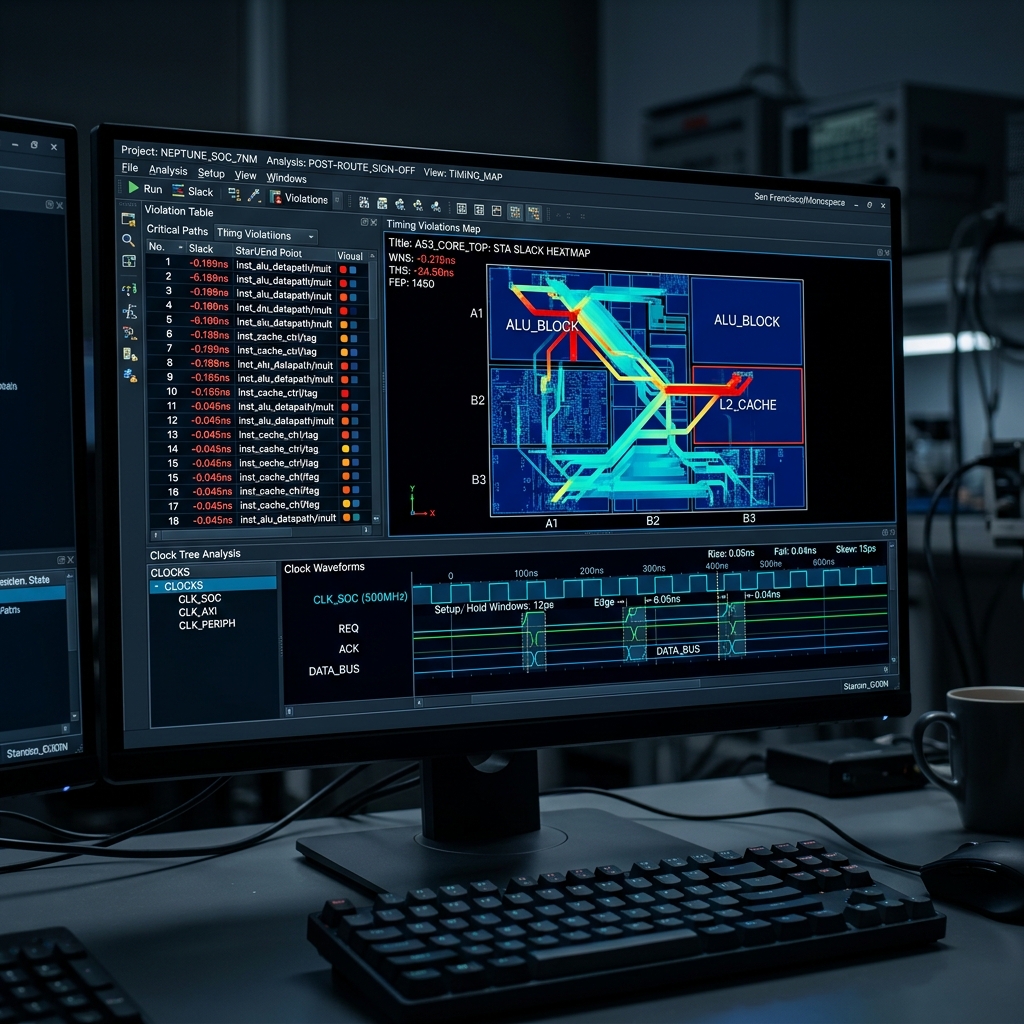
MMMC timing closure, sign-off analysis, and ECO generation to meet aggressive performance targets.
Driving Excellence in
Chip Design
Vedamsemi is a premier semiconductor consulting firm dedicated to helping global technology leaders bring complex silicon to life. With deep expertise across advanced process nodes, we bridge the gap between architectural vision and physical implementation.
Our team of expert engineers brings decades of combined experience in high-performance computing, mobile communications, and automotive electronics.
Learn More About Us
Ready to accelerate your next design cycle?
Let's discuss how our specialized engineering services can help you reach sign-off faster.
Start a Conversation